Thermal Contact Resistance - Example
In the electronic industry, chips are usually joined to substrates by
a thin layer of epoxy. Similar situations are encountered in other industries.
Modeling the epoxy layer as a separate component requires the use of a
very small element size that can result in meshing failure or an unnecessarily
large number of elements.
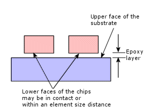
To consider the thermal resistance caused by the epoxy layer, you do
not need to model it. Thermal
contact resistance is implemented as a surface-to-surface contact
condition. You can either specify the total resistivity or the resistivity
per unit area.
Modeling Thermal Contact Resistance
There are two ways of modeling thermal contact resistance:
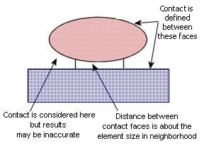
You can neglect the thin layer of epoxy when creating
the geometry. In other words, the faces of the components that are separated
by the thin layer in reality, will be touching in the model.
You can consider the thin epoxy layer when creating
the geometry. In this case there will be a gap between the faces of thermal
contact. When using this approach, there are two points to consider:
To define thermal contact resistance:
In a thermal study, right-click Connections
 and select Contact Set.
The Contact
Set PropertyManager appears.
Set Type
to Thermal Resistance.
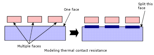
In Faces, Edges,
Vertices for Set 1  , select the desired entities
associated with one or more components.
, select the desired entities
associated with one or more components.
In Faces for
Set 2  , select the desired faces from another component.
Select Thermal
Resistance and do the following:
Set Units to the unit system you want to use.
Select Total
or Distributed and type a value.
Under Advanced,
select Node to surface or Surface to surface. The Node
to node option does not allow you to specify a thermal resistance
as connected nodes of touching faces will have the same temperature (perfect
conduction).
Click  .
.