In the electronic industry, chips are usually joined to substrates by a thin layer of epoxy. Similar situations are encountered in other industries. Modeling the epoxy layer as a separate component requires the use of a very small element size that can result in meshing failure or an unnecessarily large number of elements.
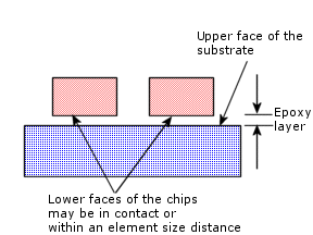
To consider the thermal resistance caused by the epoxy layer, you do not need to model it. Thermal contact resistance is implemented as a surface-to-surface contact condition.
The expected value is either the total resistance (K / W) or distributed resistance per unit area ((K * m²) / W) in the SI unit system.
The basic formula for temperature drop in a thin layer of material between two parts is given by:
ΔT = q * [t / (k * A)], where:
- DT = temperature drop at the contact zone in K
- q = heat power flowing through the contact in W
- t = thickness of the layer in m
- k = thermal conductivity of the layer material in W / (m*K)
- A = surface area of the contact in m²
The total thermal resistance is given by t / ( k* A) and the distributed resistance is given by t / k.
Modeling Thermal Contact Resistance
There are two ways of modeling thermal contact resistance:
- You can neglect the thin layer of epoxy when creating the geometry. In other words, the faces of the components that are separated by the thin layer in reality, will be touching in the model.
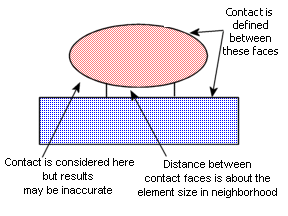
- You can consider the thin epoxy layer when creating the geometry. In this case there will be a gap between the faces of thermal contact. When using this approach, there are two points to consider:
- Results are most accurate when the distance between the two contact faces is less than or equal to the element size in the neighborhood. The below example may provide inaccurate results.
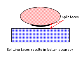
- Splitting the faces for proper pairing of thermal contact, although not necessary, improves the accuracy.
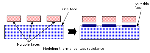
To specify different thermal resistances between a large face and a number of smaller faces, you must first split the large face to a number of smaller faces before assigning thermal contact resistance for different pairs.
Cases where Faces in the Thermal Contact Resistance are not coincident
When defining a thermal contact resistance between touching faces, it is best to use split lines to create overlapping faces between the parts. When the faces are touching but not overlapping, there are three cases. A distributed resistance Rd is understood as corresponding to a layer of material on the face in Set 1 in the cases below:
| Case 1 |
Case 2 |
Case 3 |
 |
 |
 |
| Blue face of Set 2 covers red face of Set 1. |
Red face of Set 1 covers blue face of Set 2 |
Ref Face of Set1 intersects partially blue face of Set 2 |
The total thermal resistance is: Rt = Rd / A1, where A1 is the area of the face in Set 1.
|
The total thermal resistance is Rt = Rd / A1.
Therefore, even though the face in Set 2 is smaller than the face in Set 1, the entire area of the face in Set 1 is taken into account for calculation of total resistance.
However, only the common projected area (in this case, the area of the face in Set 2) is considered to participate in heat transfer between the two faces.
|
This situation is not recommended. Use split lines to create common projected areas of contact between the faces of Set 1 and Set 2 . |